Typical Tolerances for Dimensions in Ceramic PCB Boards
Dimensions in Ceramic PCB Boards
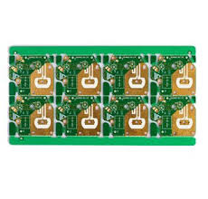
A multilayer ceramic pcb board is a specialized type of printed circuit board that uses different ceramic materials instead of traditional glass reinforced epoxy resin. This enables it to withstand higher temperatures and offer improved electrical performance. Moreover, it is able to resist harsh chemicals and provide enhanced mechanical strength and durability. These attributes make it ideal for use in situations involving extreme heat variations, microwave radio frequencies, space qualified electronics, and medical implantable devices.
The pcb manufacturing process for this variety of PCB involves applying layers of conductive and insulating materials on a substrate made from ceramic material. Then, it undergoes high-temperature firing to achieve the final product. This firing process is essential for ensuring the proper integration of the various components as well as good adhesion. The process also ensures that the copper does not oxidize, which could adversely impact its functionality.
The dimensions of a multilayer ceramic pcb board are defined by the physical size of the individual layer stacks, their thicknesses, and the distance between conductive features (such as pads and traces). To achieve optimal electrical performance, a uniform controlled impedance is required to minimize signal reflections and distortions. Conductor power density, which is influenced by the width, length, and thickness of conductive traces, is another important factor for achieving this goal.
Typical Tolerances for Dimensions in Ceramic PCB Boards
Ceramic materials have excellent electrical properties and offer better resistance to electromagnetic interference and radiation than organic PCBs. This makes them suitable for use in a wide range of applications, including wireless power transfer and charging modules, LED lighting, solar panels, and automotive sensors. They can also withstand rigorous mechanical stress and vibration. Furthermore, they are resistant to a variety of chemicals and solvents.
Despite these advantages, ceramic PCBs are more expensive than their organic counterparts, and their construction methods require more complex fabrication processes. However, advances in technology are making them more affordable and accessible to a wider range of users.
In order to ensure that the resulting multilayer ceramic pcbs meet their design goals, it is crucial for engineers to understand the basic manufacturing process of this type of board. This includes knowing the typical tolerances that are associated with these boards and incorporating them into their designs.
The first step in the process of fabricating a multilayer ceramic PCB is printing the design of the board onto a mask, which is then used to create the conductive and insulating layers. The next step is to pass the mask through a lithography system, which will create the pattern of holes for the traces and pads. This is followed by a thermal expansion chamber, which will align the ceramic substrate with silicon semiconductor chips.
Finally, the copper traces and pads are etched to expose their conductive features. These features are then soldered to the semiconductors and other components, completing the circuit. Before the finished product can be shipped to customers, it must undergo a series of tests and inspections.